![]()
![]()
![]()


Please note: wafer level TXRF measurements are no longer available, details on TXRF Home Page.
|
Please note: wafer level TXRF measurements are no longer available, details on TXRF Home Page.
|
|
|
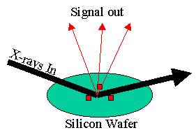
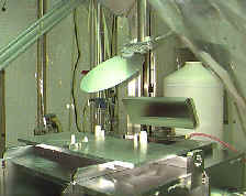
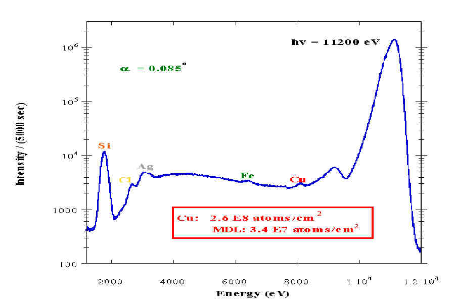
The Stanford Synchrotron Radiation Laboratory (SSRL) had established a state of the art facility to analyze trace contamination on the surface of practical silicon wafers using the technique of Total Reflection X-Ray Fluorescence (TXRF). The project started as a direct collaboration with scientists from both Intel and Hewlett Packard. The project was subsequently broadened to include Sematech member companies with the goal of developing a facility that could be used routinely by the semiconductor industry. The goal was met where semiconductor companies were able to bring full wafers (up to 200 mm) for multipoint analysis at detection limits better than 1E8 atoms/cm2. The semiconductor companies and other laboratories that participated in this project included: AMD, Applied Materials, Atominstitut, Balazs Analytical Labs, Charles Evans and Associates, DEC, Dow Chemical, Hewlett Packard, IBM, Intel, Komatsu, Lucent, MIT, Motorola, National Instruments, Rigaku, Sandia National Laboratory, Stanford University, Texas Instruments, Wacker, and Waseda University. This facility was instrumental in helping industry achieve detection limits meeting the Sematech Roadmap. By the end of the 1990's, wafers with surface metal concentrations in the low 1E8 atoms/cm2 range were becoming routinely achievable and techniques such as VPD TXRF were becoming commercially available. As a result, the need for a synchrotron-based TXRF facility that could be used for routine measurements, although desirable, was not a necessary element in continuing to meet the Sematech Roadmap. As a result, the facility described on this web page was decommissioned and replaced with a smaller system that continues to provide the capability for high sensitivity TXRF measurements for small and irregularly shaped samples rather than 200 mm wafers. Beam time for such measurements must be obtained using the standard SSRL Proposal Process. Presently, research is being conducted on samples from the NASA Genesis Sample Return Mission as well as other unique samples including surface contamination on LIGO optics and detection of catalyst particles on substrates used for nanowire growth. In addition to this TXRF system, a microprobe using Kirkpatrick-Baez optics has been added to the beam line that allows for microanalysis at micron spatial resolution.
Contact InformationPlease contact us if you have any questions regarding the SSRL TXRF program.
|
Send mail to
pianetta@stanford.edu with
questions or comments about this web site.
|